Transient beam fanning effects in fiber-like BTO-crystals, that occur if an external electric field is applied, have been studied.
Beam fanning means an asymmetrically amplified scattering. By
this process an important part of the energy of the incident signal
beam can be transferred to the fanning. This effect normally occurs
in photorefractive materials that have high values of the electrooptical
coefficients and therefore provide a high coupling gain (e.g.
BaTiO3). In sillenite type crystals (BTO) this effect
only occurs if a very high external field is applied. Therefore
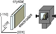
we used fiber-like [1,2,3] BTO-crystals (Fig.1).
Figure 1: Fiber-like BTO-crystals
Because of their little width (1...4 mm) high electric fields
can be applied using moderate voltages, and because of their length
(8...20 mm) the interaction area is very large.
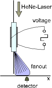
Figure 2: Experimental arrangement
These properties lead to new effects that can not be observed in bulk materials.
Fig.2 shows the experimental set-up that was used for the investigations. A square-wave voltage (U=5kV, E=50kV/cm) with low frequency (maximally some Hz) was applied. So every switching of the voltage could be considered as a single event. It turned out that the effects occur in the same way if the voltage changes its polarity of if the voltage is switched on or off [4,5]. The effect only depends on changing the electric field.
Fig.3 shows what could be seen on the screen.
The intensity pattern shows the transmitted signal beam in the
central point and the fanning in direction of the x-axis. The
fanning has the shape of a club and is not very closely concentrated
near the x-axis. The reason is that the electrooptical coefficients
of BTO are equal (unlike BaTiO3) and so the coupling
strength does not very strong depend on the direction.
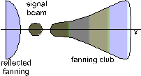
Figure 3: Image on the screen
Because of the small aperture of the crystal at the output, there
was a reflected part of the fanning at the opposite side of the
central point. It could be observed that a really strong fanning
only occurs in the moment when the applied voltage and with that
the electric field was switched.
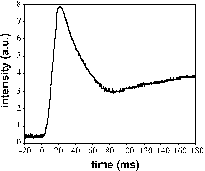
Figure 4: Course in time of the intensity of the fanning in a certain point.
The course in time of the intensity on a point shape detector
in the fanning was recorded (Fig.4).
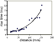
Figure 5: Build-up time of the fanning at different
positions
A peak of the intensity occurs rather fast (approximately 20 ms) after switching the voltage (at t=0). In the other time period when the electric field is stationary the fanning keeps on a much lower intensity level.
We measured the rise time of the peak (time from switching the
field till to reaching the maximum of the peak) for different
distances of the detector from the central point along the x-axis
(Fig.5).
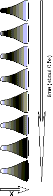
Figure 6: Temporal series of pictures of the fanning
(drawing)
The rise time increases with growing distance to the central point (according to a growing angle of the fanning with respect to the transmitted signal beam).
This means that the fanning is a chain process in this case. The energy is transferred from the signal beam to the first appearing fanning with a small angle to the signal beam, then from this part of the fanning to the next part (larger angle) and so on.
Fig.6 shows a drawn temporal series of intensity patterns of the fanning.
This way, something like a "fanning wave" can be seen moving over the screen.
The maximum intensity of the peaks (Fig.4) depends on the position
along the x-axis (Fig.7).
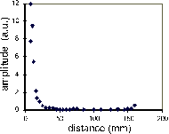
Figure 7: Peak amplitude (intensity) as a function
of the position on the x-axis
The highest intensities are obtained near the central point (according to small angles between signal beam and fanning). The intensity decreases with increasing distance.
However, a transient fanning effect has been studied experimentally.
This effect occurs in fiber-like BTO crystals when the applied
high voltage changes.
Acknowledgment
This research has been partially supported by the
Deutsche Forschungsgemeinschaft (DFG) within the Innovationskolleg
"Optische Informationstechnik" (INK 1/A1) at the Friedrich-Schiller-Universität
Jena.
References
[1] A.A. Kamshilin, E. Raita, V.V. Prokofiev, and T. Jaaskelainen, Appl. Phys. Lett. 67, 3242 (1995)
[2] A.A. Kamshilin, R. Silvennoinen, and T. Jaaskelainen, Opt. Lett. 18, 690 (1993)
[3] A.A. Kamshilin, V.V. Prokofiev, and T. Jaaskelainen, IEEE J. Quantum Electron. 31, 1642 (1995)
[4] E. Raita, A.A. Kamshilin, V.V. Prokofiev, and T. Jaaskelainen, Appl. Phys. Lett. 70, 1641 (1997)
[5] S.I. Stepanov and M.P. Petrov, Opt. Commun. 53, 292 (1985)